- 您现在的位置:买卖IC网 > Sheet目录308 > ADUM3100BRZ-RL7 (Analog Devices Inc)IC DIGITAL ISOLATOR SGL 8-SOIC
�� ��
��
��Data� Sheet�
�APPLICATIONS� INFORMATION�
�PC� BOARD� LAYOUT�
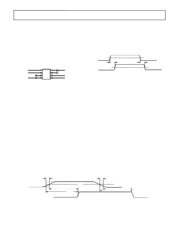
�The� ADuM3100� digital� isolator� requires� no� external� interface�
�circuitry� for� the� logic� interfaces.� A� bypass� capacitor� is�
�recommended� at� the� input� and� output� supply� pins.� The� input�
�bypass� capacitor� can� conveniently� connect� between� Pin� 3� and�
�Pin� 4� (see� Figure� 12).� Alternatively,� the� bypass� capacitor� can� be�
�located� between� Pin� 1� and� Pin� 4.� The� output� bypass� capacitor�
�ADuM3100�
�PROPAGATION� DELAY-RELATED� PARAMETERS�
�Propagation� delay� time� describes� the� length� of� time� it� takes� for� a�
�logic� signal� to� propagate� through� a� component.� Propagation�
�delay� time� to� logic� low� output� and� propagation� delay� time� to�
�logic� high� output� refer� to� the� duration� between� an� input� signal�
�transition� and� the� respective� output� signal� transition�
�(see� Figure� 13).�
�can� be� connected� between� Pin� 7� and� Pin� 8� or� Pin� 5� and� Pin� 8.�
�The� capacitor� value� should� be� between� 0.01� μF� and� 0.1� μF.� The�
�total� lead� length� between� both� ends� of� the� capacitor� and� the�
�power� supply� pins� should� not� exceed� 20� mm.�
�INPUT� (V� I� )�
�OUTPUT� (V� O� )�
�t� PLH�
�t� PHL�
�50%�
�50%�
�V� DD1�
�V� 1� (DATA)�
�V� DD2�
�(OPTIONAL)�
�Figure� 13.� Propagation� Delay� Parameters�
�V� O� (DATA� OUT)�
�GND� 1� GND� 2�
�Figure� 12.� Recommended� Printed� Circuit� Board� Layout�
�See� the� AN-1109� Application� Note� for� board� layout� guidelines.�
�SYSTEM-LEVEL� ESD� CONSIDERATIONS� AND�
�ENHANCEMENTS�
�System-level� ESD� reliability� (for� example,� per� IEC� 61000-4-x)�
�is� highly� dependent� on� system� design,� which� varies� widely� by�
�application.� The� ADuM3100� incorporates� many� enhancements�
�to� make� ESD� reliability� less� dependent� on� system� design.� The�
�enhancements� include�
�Pulse-width� distortion� is� the� maximum� difference� between� t� PLH�
�and� t� PHL� and� provides� an� indication� of� how� accurately� the� input�
�signal� timing� is� preserved� in� the� component� output� signal.�
�Propagation� delay� skew� is� the� difference� between� the� minimum�
�and� maximum� propagation� delay� values� among� multiple�
�ADuM3100� components� operated� at� the� same� operating�
�temperature� and� having� the� same� output� load.�
�Depending� on� the� input� signal� rise/fall� time,� the� measured�
�propagation� delay� based� on� the� input� 50%� level� can� vary� from�
�the� true� propagation� delay� of� the� component� (as� measured� from�
�its� input� switching� threshold).� This� is� due� to� the� fact� that� the�
�?�
�?�
�?�
�?�
�?�
�ESD� protection� cells� added� to� all� input/output� interfaces.�
�Key� metal� trace� resistances� reduced� using� wider� geometry�
�and� paralleling� of� lines� with� vias.�
�The� SCR� effect� inherent� in� CMOS� devices� minimized� by�
�use� of� guarding� and� isolation� techniques� between� PMOS�
�and� NMOS� devices.�
�Areas� of� high� electric� field� concentration� eliminated� using�
�45°� corners� on� metal� traces.�
�Supply� pin� overvoltage� prevented� with� larger� ESD� clamps�
�between� each� supply� pin� and� its� respective� ground.�
�input� threshold,� as� is� the� case� with� commonly� used� optocouplers,�
�is� at� a� different� voltage� level� than� the� 50%� point� of� typical� input�
�signals.� This� propagation� delay� difference� is�
�Δ� LH� =� t� ′� PLH� ?� t� PLH� =� (� t� r� /0.8� V� I� )(0.5� V� 1� ?� V� ITH� (L-H)� )�
�Δ� HL� =� t� ′� PHL� ?� t� PHL� =� (� t� f� /0.8� V� I� )(0.5� V� 1� ?� V� ITH� (H-L)� )�
�where:�
�t� PLH� ,� t� PHL� are� propagation� delays� as� measured� from� the� input�
�50%.�
�t� ′� PLH� ,� t� ′� PHL� are� propagation� delays� as� measured� from� the� input�
�switching� thresholds.�
�While� the� ADuM3100� improves� system-level� ESD� reliability,� it�
�is� no� substitute� for� a� robust� system-level� design.� See� Application�
�t� r� ,� t� f� are� input� 10%� to� 90%� rise/fall� time.�
�Note� AN-793,� ESD/Latch-Up� Considerations� with� i� Coupler�
�V� I� is� the� amplitude� of� input� signal� (0�
�to� V� I� levels� assumed).�
�Isolation� Products� for� detailed� recommendations� on� board�
�layout� and� system-level� design.�
�V� ITH� (L–H)� ,� V� ITH� (H–L)� are� input� switching� thresholds.�
�V� ITH(L–H)�
�V� I�
�?� LH�
�50%�
�?� HL�
�V� ITH(H–L)�
�INPUT� (V� I� )�
�t� PLH�
�t'� PLH�
�t� PHL�
�t'� PHL�
�OUTPUT� (V� O� )�
�50%�
�Figure� 14.� Impact� of� Input� Rise/Fall� Time� on� Propagation� Delay�
�Rev.� C� |� Page� 13� of� 16�
�发布紧急采购,3分钟左右您将得到回复。
相关PDF资料
ADUM3160BRWZ-RL
IC ISOLATOR USB 2.5K 16SOIC
ADUM3201WCRZ
ISOLATOR DGTL 25MBPS 2CH 8SOIC
ADUM3210WCRZ
IC DIGITAL ISOLATOR 2CH 8-SOIC
ADUM3300CRWZ
IC DIGITAL ISOLATOR 3CH 16-SOIC
ADUM3400BRWZ
IC DIGITAL ISOLATOR 4CH 16-SOIC
ADUM3442CRWZ-RL
IC DIGITAL ISOLATOR 4CHAN 16SOIC
ADUM4223BRWZ
ISOLATOR DIGITAL
ADUM4402CRWZ
IC DIGITAL ISOLATOR 4CH 16-SOIC
相关代理商/技术参数
ADUM3123ARZ
功能描述:4A Gate Driver Magnetic Coupling 3000Vrms 1 Channel 8-SOIC 制造商:analog devices inc. 系列:iCoupler? 包装:管件 零件状态:有效 技术:磁耦合 通道数:1 电压 - 隔离:3000Vrms 共模瞬态抗扰度(最小值):50kV/μs 传播延迟 tpLH / tpHL(最大值):68ns,68ns 脉宽失真(最大):- 上升/下降时间(典型值):12ns,12ns 电流 - 输出高,低:- 电流 - 峰值输出:4A 电压 - 正向(Vf)(典型值):- 电流 - DC 正向(If):- 电压 - 电源:4.5 V ~ 18 V 工作温度:-40°C ~ 125°C 安装类型:表面贴装 封装/外壳:8-SOIC(0.154",3.90mm 宽) 供应商器件封装:8-SOIC 认可:CSA,UR,VDE 标准包装:98
ADUM3123ARZ-RL7
功能描述:4A Gate Driver Magnetic Coupling 3000Vrms 1 Channel 8-SOIC 制造商:analog devices inc. 系列:iCoupler? 包装:带卷(TR) 零件状态:有效 技术:磁耦合 通道数:1 电压 - 隔离:3000Vrms 共模瞬态抗扰度(最小值):50kV/μs 传播延迟 tpLH / tpHL(最大值):68ns,68ns 脉宽失真(最大):- 上升/下降时间(典型值):12ns,12ns 电流 - 输出高,低:- 电流 - 峰值输出:4A 电压 - 正向(Vf)(典型值):- 电流 - DC 正向(If):- 电压 - 电源:4.5 V ~ 18 V 工作温度:-40°C ~ 125°C 安装类型:表面贴装 封装/外壳:8-SOIC(0.154",3.90mm 宽) 供应商器件封装:8-SOIC 认可:CSA,UR,VDE 标准包装:1,000
ADUM3123BRZ
功能描述:4A Gate Driver Magnetic Coupling 3000Vrms 1 Channel 8-SOIC 制造商:analog devices inc. 系列:iCoupler? 包装:管件 零件状态:有效 技术:磁耦合 通道数:1 电压 - 隔离:3000Vrms 共模瞬态抗扰度(最小值):50kV/μs 传播延迟 tpLH / tpHL(最大值):62ns,62ns 脉宽失真(最大):- 上升/下降时间(典型值):12ns,12ns 电流 - 输出高,低:- 电流 - 峰值输出:4A 电压 - 正向(Vf)(典型值):- 电流 - DC 正向(If):- 电压 - 电源:7.4 V ~ 18 V 工作温度:-40°C ~ 125°C 安装类型:表面贴装 封装/外壳:8-SOIC(0.154",3.90mm 宽) 供应商器件封装:8-SOIC 认可:CSA,UR,VDE 标准包装:98
ADUM3123BRZ-RL7
功能描述:4A Gate Driver Magnetic Coupling 3000Vrms 1 Channel 8-SOIC 制造商:analog devices inc. 系列:iCoupler? 包装:带卷(TR) 零件状态:有效 技术:磁耦合 通道数:1 电压 - 隔离:3000Vrms 共模瞬态抗扰度(最小值):50kV/μs 传播延迟 tpLH / tpHL(最大值):62ns,62ns 脉宽失真(最大):- 上升/下降时间(典型值):12ns,12ns 电流 - 输出高,低:- 电流 - 峰值输出:4A 电压 - 正向(Vf)(典型值):- 电流 - DC 正向(If):- 电压 - 电源:7.4 V ~ 18 V 工作温度:-40°C ~ 125°C 安装类型:表面贴装 封装/外壳:8-SOIC(0.154",3.90mm 宽) 供应商器件封装:8-SOIC 认可:CSA,UR,VDE 标准包装:1,000
ADUM3123CRZ
功能描述:4A Gate Driver Magnetic Coupling 3000Vrms 1 Channel 8-SOIC 制造商:analog devices inc. 系列:iCoupler? 包装:管件 零件状态:有效 技术:磁耦合 通道数:1 电压 - 隔离:3000Vrms 共模瞬态抗扰度(最小值):50kV/μs 传播延迟 tpLH / tpHL(最大值):62ns,62ns 脉宽失真(最大):- 上升/下降时间(典型值):12ns,12ns 电流 - 输出高,低:- 电流 - 峰值输出:4A 电压 - 正向(Vf)(典型值):- 电流 - DC 正向(If):- 电压 - 电源:11.1 V ~ 18 V 工作温度:-40°C ~ 125°C 安装类型:表面贴装 封装/外壳:8-SOIC(0.154",3.90mm 宽) 供应商器件封装:8-SOIC 认可:CSA,UR,VDE 标准包装:98
ADUM3123CRZ-RL7
功能描述:4A Gate Driver Magnetic Coupling 3000Vrms 1 Channel 8-SOIC 制造商:analog devices inc. 系列:iCoupler? 包装:带卷(TR) 零件状态:有效 技术:磁耦合 通道数:1 电压 - 隔离:3000Vrms 共模瞬态抗扰度(最小值):50kV/μs 传播延迟 tpLH / tpHL(最大值):62ns,62ns 脉宽失真(最大):- 上升/下降时间(典型值):12ns,12ns 电流 - 输出高,低:- 电流 - 峰值输出:4A 电压 - 正向(Vf)(典型值):- 电流 - DC 正向(If):- 电压 - 电源:11.1 V ~ 18 V 工作温度:-40°C ~ 125°C 安装类型:表面贴装 封装/外壳:8-SOIC(0.154",3.90mm 宽) 供应商器件封装:8-SOIC 认可:CSA,UR,VDE 标准包装:1,000
ADUM3150ARSZ
功能描述:SPI Digital Isolator 3750Vrms 6 Channel 40Mbps 25kV/μs CMTI 20-SSOP (0.209", 5.30mm Width) 制造商:analog devices inc. 系列:iCoupler?,SPIsolator? 包装:管件 零件状态:有效 技术:磁耦合 类型:SPI 隔离式电源:无 通道数:6 输入 - 输入侧 1/输入侧 2:4/2 通道类型:单向 电压 - 隔离:3750Vrms 共模瞬态抗扰度(最小值):25kV/μs 数据速率:40Mbps 传播延迟 tpLH / tpHL(最大值):25ns,25ns 脉宽失真(最大):2ns 上升/下降时间(典型值):2.5ns,2.5ns 电压 - 电源:3 V ~ 5.5 V 工作温度:-40°C ~ 125°C 封装/外壳:20-SSOP(0.209",5.30mm 宽) 供应商器件封装:20-SSOP 标准包装:66
ADUM3150ARSZ-RL7
功能描述:SPI Digital Isolator 3750Vrms 6 Channel 40Mbps 25kV/μs CMTI 20-SSOP (0.209", 5.30mm Width) 制造商:analog devices inc. 系列:iCoupler?,SPIsolator? 包装:剪切带(CT) 零件状态:有效 技术:磁耦合 类型:SPI 隔离式电源:无 通道数:6 输入 - 输入侧 1/输入侧 2:4/2 通道类型:单向 电压 - 隔离:3750Vrms 共模瞬态抗扰度(最小值):25kV/μs 数据速率:40Mbps 传播延迟 tpLH / tpHL(最大值):25ns,25ns 脉宽失真(最大):2ns 上升/下降时间(典型值):2.5ns,2.5ns 电压 - 电源:3 V ~ 5.5 V 工作温度:-40°C ~ 125°C 封装/外壳:20-SSOP(0.209",5.30mm 宽) 供应商器件封装:20-SSOP 标准包装:1